ABOUT
S.A.V.E.D. was founded by Sophie BOUAT, Ph.D in Physics & Engineer in Material Physics.
R&D manager at ENERBEE (2016-2018)
AVSIS (2014-2015)
Polygon Physics (2012-2013)
S.A.V.E.D. was founded by Sophie BOUAT, Ph.D in Physics & Engineer in Material Physics.
R&D manager at ENERBEE (2016-2018)
AVSIS (2014-2015)
Polygon Physics (2012-2013)
A scanning electron microscope (SEM) is a type of electron microscope that produces images of a sample by scanning the surface with a focused beam of electrons. The electrons interact with atoms in the sample, producing various signals that contain information about the surface topography and composition of the sample. The electron beam is scanned in a raster scan pattern, and the position of the beam is combined with the detected signal to produce an image. SEM can achieve resolution better than 1 nanometer. Specimens are observed in high vacuum in conventional SEM, or in low vacuum or wet conditions in variable pressure or environmental SEM, and at a wide range of cryogenic or elevated temperatures with specialized instruments.
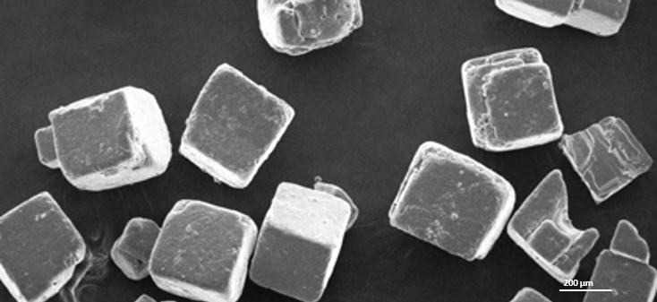
The most common SEM mode is the detection of secondary electrons emitted by atoms excited by the electron beam. The number of secondary electrons that can be detected depends, among other things, on specimen topography. By scanning the sample and collecting the secondary electrons that are emitted using a special detector, an image displaying the topography of the surface is created.
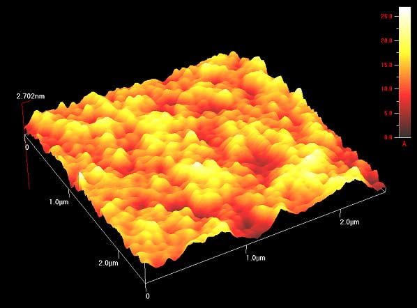
AFM is a type of scanning probe microscopy (SPM), with demonstrated resolution on the order of fractions of a nanometer, more than 1000 times better than the optical diffraction limit. The information is gathered by “feeling” or “touching” the surface with a mechanical probe. Piezoelectric elements that facilitate tiny but accurate and precise movements on (electronic) command enable precise scanning.
The AFM has three major abilities : force measurement, imaging, and manipulation.
In force measurement, AFMs can be used to measure the forces between the probe and the sample as a function of their mutual separation. This can be applied to perform force spectroscopy, to measure the mechanical properties of the sample, such as the sample’s Young’s modulus, a measure of stiffness.
For imaging, the reaction of the probe to the forces that the sample imposes on it can be used to form an image of the three-dimensional shape (topography) of a sample surface at a high resolution. This is achieved by raster scanning the position of the sample with respect to the tip and recording the height of the probe that corresponds to a constant probe-sample interaction (see section topographic imaging in AFM for more details). The surface topography is commonly displayed as a pseudocolorplot.
In manipulation, the forces between tip and sample can also be used to change the properties of the sample in a controlled way. Examples of this include atomic manipulation, scanning probe lithography and local stimulation of cells.
Simultaneous with the acquisition of topographical images, other properties of the sample can be measured locally and displayed as an image, often with similarly high resolution. Examples of such properties are mechanical properties like stiffness or adhesion strength and electrical properties such as conductivity or surface potential. In fact, the majority of SPM techniques are extensions of AFM that use this modality.